Because Over-Engineering is Underrated
MCU Relay Control Power System
Spinning Jenny Custom Manufacturing is engaged in developing an IoT system intended to bring some leading-edge commercial capabilities into a residential setting. The system integrates a variety of sensors and uses locally trained machine learning models running on resource-constrained hardware to optimize system operation based on local data.
Fortunately, the system can minimize computational requirements by training on predicting residual error in a physics-based equation model rather than attempting to predict outcomes directly from raw sensor data. This significantly reduces the complexity of the machine learning problem while still allowing the system to adapt to local conditions.
One of the system goals is complete local autonomy. Jenny is deeply suspicious of cloud-dependent IoT products. The only thing that irritates her more than squirrels is an IoT startup that requires a subscription to use bought and paid for equipment, or worse, one that performs their processing in the cloud, goes bankrupt, and consequently bricks a perfectly functional piece of hardware because someone stopped paying their AWS bill.
So the complicated part of the project is the software. The hardware's job is relatively straightforward: run the software, and read sensors, report their values, and close relays when instructed. However, the device is intended to operate for extended periods without supervision, which means reliability is critical. A homeowner shouldn't have to visit the utility room every few days to press a reset button.
Unfortunately, the system's otherwise simple hardware requirements create several places noise and chaos can pop up. Analog power systems and digital devices get along like, well, dogs and cats.
PROBLEM STATEMENT
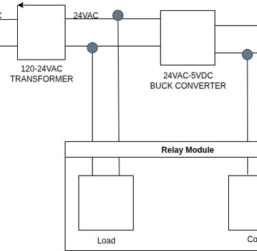
The controller communicates via standard 802.11 WiFi for configuration and remote access, while remote sensor nodes communicate using the ESP-NOW WiFi protocol, with its longer range and lower power requirements. The hardware also drives several relays controlling 24VAC solenoids located at the end of relatively long wire runs.
While 24VAC control hardware is inexpensive and reliable, inductive loads are notorious for generating electrical noise. Relay transitions can introduce voltage transients and conducted noise that may interfere with RF communications or contaminate the MCU power rail. Additionally, while the MCU contains an onboard voltage regulator, sufficient voltage sag on the 5V rail will still trigger a brownout reset.

The relevant design goals for the power and relay systems were:
Provide 24 VAC to the downstream solenoids
Isolate the digital control electronics from the relay and solenoid circuitry, to prevent power drops, inductive kickback and relay noise from affecting MCU operation.
Maintain stable MCU power and isolate the MCU from transients as displays refresh, indicators change state, buttons are pressed, and peripherals become active.
Prevent brownout resets during high-current activities such as OTA firmware updates.
Maintain a HIGH means YES/ON logic convention at the MCU input and outputs.
As a fail-safe for MCU malfunction, have the relay inputs be HIGH by default (at power-on) since the relay module is active low, and we don't want them to activate if the MCU forgets to power up when the system is turned on.
AoA: ANALYSIS OF ALTERNATIVES
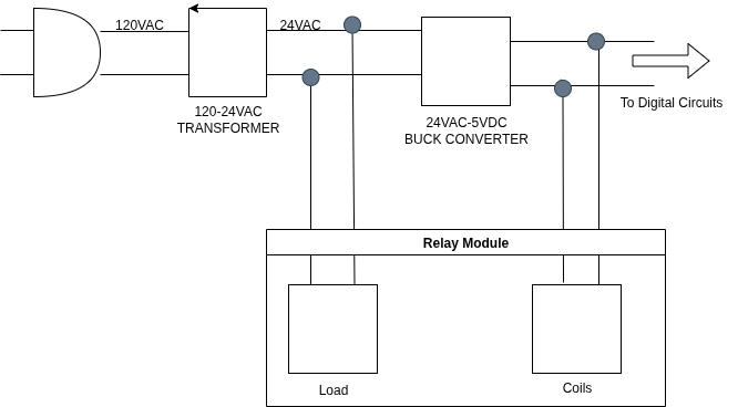
One option was to power the digital electronics from a completely separate supply. The relay side would be fed from a 120VAC to 24VAC transformer, while the digital side would receive power from a dedicated 120VAC-to-5VDC converter plugged into a second wall outlet. That would have been electrically simple, but it was awkward and unexpected in a piece of residential equipment, and violated the design principle of least annoyance: A homeowner is unlikely to appreciate giving up a second receptacle or having to make another run to Home Depot for a splitter. So tapping the 24VAC in for the digital side was the way to go.
Another option was to use a separate converter for each control side - one for the 5VDC requirement for the relay side, a second one for the 5VDC optoisolator and indicator LEDs and MCU, and a third for the 3.3VDC button (and later, potentially sensor) inputs and the OLEDs we're using for local device programming (required by the choice of ESP32-S3 MCU, which has 3.3V GPIO pins.) Since we were using buck converters to get from 24VAC to 5VDC, that would have been bulky and expensive (and overkill for a power budget that could be measured in 100s of mA on each rail), especially since normal buck converters would share a common reference, and so would not provide galvanic isolation. We'd have to use isolated buck converters, increasing our expense, and, unless we used a fourth converter, that would still leave the MCU on the same rail as the LEDs, including the optoisolator LEDs that would be quite close to the relays. So that approach was out too. Isolators and filtering seemed to be the right approach.
SOLUTION DEVELOPMENT
POWER BUDGET:
Spinning Jenny's solution started with a power budget for each rail:
The 5VDC relays we're using draw 70mA when activated, and may draw 80mA as they activate. While the application will only use one relay (two maximum possible in a future release; more than that at a time risks causing downstream damage to the equipment on the other side of the solenoids), our approach supports a worst case of all relays activated for a total draw of between 560-640mA.
The ESP32-S3 spec'ed as the MCU draws 30-110mA in normal operation, but can peak to up to 385mA during sustained WiFi operations - we budgeted for a worse than worst case 500+mA to ensure no resets or glitches during simultaneous heavy WiFi and firmware operations.
When a relay channel is active, there's both a optoisolator LED and an indicator LED active. Again, a maximum of two channels will be active, but we budgeted for all 8 being active at once. Slightly less than 20mA for the optocoupler and about the same for the indicator LED gives us 40mA per channel, for 320mA. Button draw is negligible, since they're connected to the MCU through a Schmitt converter with very high impedance inputs. There are two 0.96" OLEDS (one for menu and programming, and the other for status.) At worst case (full white), they draw 30mA at 3.3V, so 60mA total. That gives a combined I/O current requirement of 380mA.
Plus 120mA of "parasitic" current loss to protect the isolation design (of which more later).
Total worst case current draw is right around 1.6A. The buck converter is rated at 2.2A of continuous current at 5VDC, with a peak output of 3A (briefly, according to the datasheet, and the system is designed to never have to answer the question how long is briefly), plenty to power all the downstream digital devices and the relay, with over 30% headroom for the buck converter to drop from its rated output (due to heat, upstream power quality, or just bad luck) even if all eight relays activated and both OLEDs went solid white in the middle of an OTA update. That meant getting to a single 5VDC power converter seemed to be the right move, presuming we could design the right distribution, filtering, and isolation approach.
DESIGN APPROACH
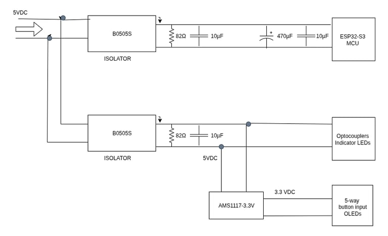
Steve decided to use a split rail, ground-shared, isolated DC-DC (or, more accurately, ground partially shared DC-DC-DC-DC) approach: The 5VDC side of the buck converter splits in parallel into three rails via a terminal block. The first rail feeds the relay coil side of the relay module. We expect that power to be dirty, and we expect the relays not to care. Each of the other two feeds goes into a B0505S-3WR3, each acting as a safety isolator that protects its rail from dirty power caused by the buck convertor and / or relays. We split into two feeds because the rated current for each B0505S is 600mA. One B0505S regulator would probably have been fine, but using our worst case power budget, if the I/O requirements shot to 380mA while the MCU was using 385mA on radio communications, we could overload a single regulator. That's the kind of event that never happens during bench testing - only at a customer site at 2am on a Saturday. Two of them in concert provide a safety margin in current draw.
Each digital rail (the two 5VDC rails and the downstream 3.3VDC rail behind the twin B0505S isolaters) shares a common star ground, but does not share a ground with either the AC side of the power supply or the relay coil rail. That maintains isolation between the dirty relay power rail and the clean digital power rails while providing a common digital reference for the digital circuitry. Because everything on the digital side is behind the two isolaters at this point, the lack of galvanic isolation between the digital rails is not an issue.
Note that the MCU is not powering anything but itself and the signal on its GPIO pins, and with the exception of the OLED screens on the I2C pins, its IO pins are not directly connected to any powered components. The buttons circuits are tied HIGH to the 3.3V rail through a 10kΩ resistor. When the button is depressed, it opens a circuit to ground in series with a 1kΩ resistor and in parallel with a 0.1µF capacitor (for analog debounce) driving the circuit LOW. Each button circuit attaches to its respective GPIO pin through a Schmitt inverter, so when the button circuit goes LOW, the Schmitt inverter places a HIGH (3.3V) signal on the GPIO pin.
The GPIO output to activate the optocouplers and indicator LEDs is fed through a ULN2803, so when a pin goes HIGH, it opens a path to ground for the active low optoisolaters and for the indicator LEDs. The indicator LEDs are tied to 5VDC through 150Ω resistors, so they illuminate when the Darlington opens to ground. That approach also means the relay control circuitry defaults to a safe OFF state without requiring special startup code. If a future MCU has different GPIO initialization behavior than the ESP32, we won't have to rely on software to prevent unintended relay activation during startup.
We added RC snubbers across the common and normally open relay contacts to minimize inductive kick and noise from the solenoids (amplified by the distance between the solenoids and the relays). And, probably more suspenders than belt, we added a 100nF decoupling capacitor between GND and VCC on both the Darlington and Schmitt converter. Also, the plan is to physically design the enclosure with the 24VAC input, the relay module and buck converter on one side, and a few inches of separation between it and the digital circuitry, connected by a ribbon cable carrying the control signals and 5VDC power. A little physical separation between the noisy side and the sensitive side can be worth as much as another page of parts on the bill of materials.
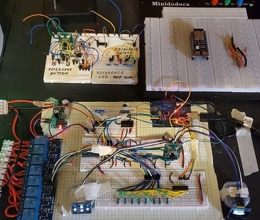
Power System Front End
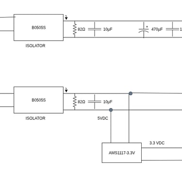
Because we have the margin, and because the B0505S is an unregulated isolater, we're using a 82Ω/2W watt resistor in parallel to provide a preload, ensuring that the B0505S always sees 10% of its rated current (the datasheet says the R3 is fine at 5%, if you want to believe datasheets.) (We're running on wall power, so battery life isn't a consideration, and a quick back of the envelope calculation indicates 60mA at 5VDC is about 5.25 kWh per year. At current average residential electricity rates, that's 80 cents a year, or one Starbucks Double Foam Venti Latte a decade. Life is about priorities, isn't it?) Each B0505S also has a 10 µF 50VDC rated ceramic capacitor in parallel to filter high and midrange frequency ripples.
One B0505S feeds the only the MCU via its 5V pin (which is regulated down to 3.3V by the board's built-in SGM2212, so the unregulated nature of the isolator isn't a factor here). That feed has a 470µF electrolytic capacitor across the ESP-32 5V and ground input pins to smooth out any transient response gap from the isolator (the B0505S has a fairly slow transient response, so giving the MCU a few milliseconds of dropout coverage - for example, at the beginning of a transmission - makes sense.),There's also a second 10 µF ceramic capacitor the MCU. We chose the two 10µF capacitors at opposite ends of the trace instead of a single 22µF capacitor so that we could place one next to the regulator outputs and one next to the MCU power inputs. On the breadboard, it didn't make much difference, but looking ahead to a PCB, the several inches between the power output and the MCU could have created inductive coupling with the single capacitor near the power supply.
The second B0505S feeds the 5VDC output rail, which supplies the indicator LEDs and optocouplers. It also feeds an AMS1117-3.3V LDO (yes, it's less efficient than a switching regulator, but it's a smaller, simpler component, and at these loads it's fine - and the efficiency loss isn't significant on wall power anyway.) The AMS1117 in turn feeds the 3.3VDC button input system and two 0.96" OLEDS - which have built-in power capacitors, saving us a 10µF capacitor across each screen. Everything on this rail handle a little voltage variation, so there's no 5VDC regulator inline.
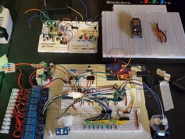
Power System Back End
Digital Circuits Power System
RESULTS
In terms of design goals, the circuit and physical design seems to be effective:
The relay block manages provision of 24VAC to the downstream solenoids, while 5VDC from the buck converter powers the coils. Everything else is behind isolaters.
The two B0505S isolaters give us galvanic separation of the digital circuitry from the dirty relay coil power, the built in optocouplers and flyback diodes on the relay module provide, respectively, galvanic separation of the signals and suppression of inductive transients at their source.
Using two isolaters provides enough headroom to maintain stable MCU power and prevent brownouts during wireless communications. The 470µF capacitor protects against a few milliseconds of transient dropout while the B0505S adjust to the load, and the 10µF capacitors smooth out any transient ripples .
The separate power rails and the Schmitt converter and Darlington approach ensure that the MCU's power system and GPIO pins are isolated from local load transients.
And HIGH means YES, everywhere in the system. We don't depend on the MCU to get us to an all relay coils de-energized state - that's the natural resting position of the system.
After all that, applying power to the prototype system was anticlimactic - all the magic smoke stayed inside the components, and there was 5VDC where there was supposed to be 5VDC and 3.3VDC where there was supposed to be 3.3VDC. Scoping the rails revealed minimal transients, even when wireless communication was initiated with all 8 relays activated. No dropouts and no resets. But then, there almost never are problems on the bench. Whether the fever pitch of paranoia in designing the power system was justified will only become apparent after the system is field tested - as will the answer to the age-old question, was this design paranoid enough?